Program Overview
| Program Name | VLSI Design |
| Domain / Stream | VLSI |
| Duration | 1 Month (4 Weeks) |
| Mode | Online (Self-Paced + Weekly Tasks) |
| Certificate | Yes — MSME & ISO 9001:2015 Certified |
| Program Fee | ₹999 ₹499 50% OFF (One-Time) |
| Student Rating | ★★★★★ 4.8 / 5 by 1000+ students |
| Offer Letter | Issued on Enrollment |
| Issued By | Shiva Tech Innovations (UDYAM-WB-14-0205610) |
Program Details & Curriculum
VLSI Design Internship
Duration: 30 Days | Certificate: MSME Recognized | Support: support@vidyawan.in
Program Overview
This internship takes students through the complete real-world VLSI design lifecycle — from understanding how silicon chips are manufactured to designing, verifying, and integrating digital hardware systems using Verilog and industry-style workflows.
Students do not just learn syntax. They learn how actual semiconductor engineers think, debug, optimize, and validate hardware before fabrication.
Every level is guided by VIDYA, our AI Teacher, which evaluates answers, identifies weak concepts, provides personalised feedback, and ensures the student understands each stage before progressing.
The internship is designed around the same engineering mindset used in semiconductor companies working on CPUs, GPUs, SoCs, AI accelerators, networking chips, and embedded hardware systems.
Content Standard — How Every Topic is Taught
This internship follows a fixed learning architecture across every module so students build conceptual understanding instead of memorising Verilog syntax.
| Stage | What Happens |
|---|---|
| Concept First | Core hardware theory is explained before any coding begins |
| Demonstration | Real waveform examples, RTL diagrams, and silicon-level interpretations are shown |
| Guided Practice | Students implement logic themselves while VIDYA provides hints and correction guidance |
| Assessment | MCQ, debugging, timing, and logic questions evaluated instantly by VIDYA |
| Revision and Lock | Critical concepts reinforced through repetition and recall exercises |
| Advanced Application | Edge cases, timing failures, verification issues, and optimisation trade-offs explored |
| Real-World Connect | Every topic linked to how actual semiconductor companies use it in production |
VIDYA AI operates throughout all seven stages — checking understanding, detecting misconceptions, simplifying difficult concepts, and guiding students through debugging without directly giving solutions.
Content Quality — The Vidya Standard
The content inside every VLSI zone is written to a defined engineering standard. It is not copied from textbook PDFs or generic Verilog tutorials. It is written for Indian engineering students preparing for internships, placements, and real semiconductor industry workflows.
| Criteria | What It Means in Practice |
|---|---|
| India-Localised Examples | Concepts connected to systems students use daily — UPI machines, Jio towers, IRCTC ticketing, metro gate controllers, smart TVs, routers, biometric attendance systems |
| Interactive Verilog Practice | Every RTL example produces meaningful waveform output. Students build ALUs, traffic light controllers, FIFOs, digital locks, vending machines, UART modules, and processor blocks |
| Real Engineering Debugging | Students analyse broken RTL, failing simulations, race conditions, setup violations, incorrect waveforms, and timing failures |
| Simulation-Driven Learning | Every concept is demonstrated using waveform analysis, clock behavior, and testbench execution instead of static theory alone |
| Cultural Relevance | Analogies based on Tatkal booking load, metro rush-hour queues, hostel Wi-Fi congestion, IPL scoreboard updates, and traffic signal timing |
| Language | Clean, simple English understandable across Chennai, Kolkata, Hyderabad, Kochi, Pune, Bhubaneswar, Ahmedabad, and Guwahati |
| Length Discipline | Explanations remain concise, high-retention, and interview-focused |
| Industry Vocabulary | Students become comfortable with terms like RTL, synthesis, STA, slack, timing closure, DRC, LVS, netlist, critical path, and tapeout |
| Concept-to-Silicon Mapping | Every Verilog construct is explained in terms of actual hardware behavior — gates, flip-flops, multiplexers, datapaths, and storage elements |
| Portfolio-Focused Learning | Every project is structured to become a portfolio-ready VLSI design and verification showcase |
Curriculum — 6 Levels
LEVEL 1 — Thinking in Silicon: How Chips Are Actually Made
Real-world context: Before writing a single line of Verilog, understand what a chip really is, how fabrication works, and why hardware engineering is fundamentally different from software development.
| Module | What You Learn |
|---|---|
| From Sand to Silicon: The Chip Manufacturing Pipeline | Wafer fabrication, CMOS basics, lithography, dies, packaging, fabrication flow, process nodes |
| The VLSI Design Flow: Your Day-to-Day as a Chip Engineer | RTL design, synthesis, place-and-route, timing closure, signoff, tapeout workflow |
LEVEL 2 — Speaking Verilog: The Language of Hardware
Real-world context: Verilog is the foundation of digital hardware design. Every processor, controller, and accelerator begins as RTL.
| Module | What You Learn |
|---|---|
| Verilog Fundamentals: Modules, Ports, and Signals | Modules, wires, regs, procedural blocks, combinational RTL, synthesizable design |
| Combinational vs Sequential Logic | Flip-flops, clocks, synchronous design, setup/hold timing, sequential behavior |
LEVEL 3 — Building Blocks: The Circuits Inside Every Chip
Real-world context: Modern processors are built from reusable digital building blocks connected together at scale.
| Module | What You Learn |
|---|---|
| Arithmetic Circuits: Adders, Subtractors, and ALUs | Full adders, ripple carry, carry lookahead, ALU design, datapath fundamentals |
| Memory Elements: Registers, FIFOs, and Register Files | Storage hierarchy, FIFOs, register design, pointer logic, buffering systems |
LEVEL 4 — Verification: Proving Your Design Works
Real-world context: Verification consumes the majority of engineering effort in semiconductor companies because a fabricated bug is extremely expensive.
| Module | What You Learn |
|---|---|
| Testbench Writing and Verification Fundamentals | Stimulus generation, assertions, self-checking testbenches, DUT validation |
| Simulation and Waveform Debugging | VCD analysis, waveform interpretation, race conditions, debugging failing RTL |
LEVEL 5 — Timing, Power, and Silicon Constraints
Real-world context: A design passing simulation is not enough. Real chips must satisfy timing, power, and manufacturability constraints.
| Module | What You Learn |
|---|---|
| Static Timing Analysis and Timing Closure | Critical path analysis, slack, setup/hold violations, STA reports |
| Power Analysis and Low-Power Design | Dynamic power, leakage, clock gating, voltage scaling, power optimisation |
LEVEL 6 — Capstone: Building a Complete Digital System
Real-world context: Students integrate everything learned into a complete industry-style digital design project.
| Module | What You Learn |
|---|---|
| System-Level Integration | Top-level hierarchy, module integration, interfaces, bus design |
| Tapeout Readiness and Signoff Checks | DRC, LVS, signoff methodology, silicon validation flow |
Industry Projects
Students must complete any 2 of the 5 projects below independently and publish them on LinkedIn as portfolio projects.
| # | Project | Skills Applied |
|---|---|---|
| 1 | 4-bit ALU Design and Verification | Verilog RTL, arithmetic circuits, simulation, verification |
| 2 | Synchronous FIFO with Full/Empty Flags | Sequential logic, buffering, pointer logic, testbench design |
| 3 | Traffic Light Controller (FSM-Based) | Finite State Machines, timing logic, sequential systems |
| 4 | Simple RISC Processor (3-Instruction CPU) | Processor architecture, datapath, control logic, memory integration |
| 5 | Full Chip Signoff Simulation Report | System integration, verification methodology, timing analysis |
Minimum 2 approved project submissions are required for certification eligibility.
What Makes This Internship Different
| Traditional Courses | This Internship |
|---|---|
| Focus only on Verilog syntax | Focus on complete chip design thinking |
| Generic toy examples | Real engineering-style hardware systems |
| No verification depth | Dedicated verification and debugging workflow |
| No timing awareness | STA and timing closure included |
| No industry connection | Every topic mapped to real semiconductor workflows |
| Passive watching | Guided implementation with AI feedback |
| Theory-heavy | Simulation-driven practical learning |
Tools and Engineering Workflow Students Use
Students work with the same categories of workflows used in real digital design environments.
| Area | Concepts and Tools |
|---|---|
| RTL Design | Verilog HDL, module hierarchy, synthesizable coding |
| Simulation | Testbench writing, waveform analysis, VCD debugging |
| Verification | Assertions, self-checking logic, corner case testing |
| Timing Analysis | Slack analysis, critical path reasoning |
| System Design | ALUs, FIFOs, FSMs, processor datapaths |
| Signoff Awareness | DRC, LVS, layout validation concepts |
Certification
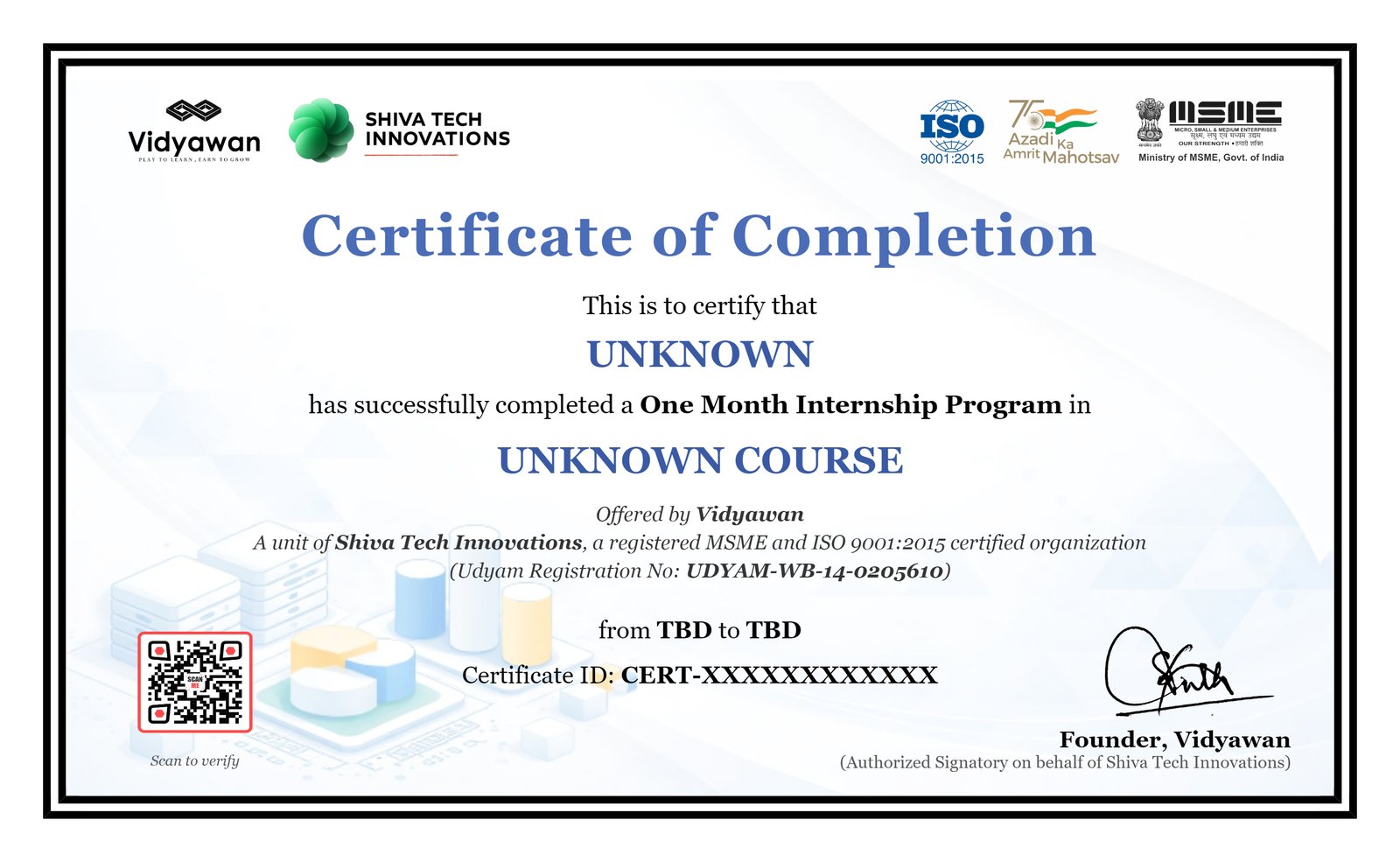
After successful project submission review and approval by the admin team, the student's MSME recognized internship certificate is generated and made available directly through the dashboard.
Internship Timeline
| Phase | Days | What Happens |
|---|---|---|
| Learning Phase | Day 1 to Day 7 | Complete all 6 learning levels |
| Project Phase | Day 8 to Day 29 | Build projects, publish on LinkedIn, submit reports and simulation outputs |
| Certification Phase | Day 30 | Project verification and certificate issuance |
Real Industry Alignment
The internship is intentionally structured around the same progression followed inside semiconductor engineering teams:
Understand silicon → Write RTL → Build circuits → Verify behavior → Close timing → Integrate systems → Prepare for tapeout
By the end of the internship, students are expected to:
- Read and write synthesizable Verilog
- Design and debug digital systems
- Create verification testbenches
- Interpret timing and waveform issues
- Understand real chip design constraints
- Build portfolio-ready VLSI projects suitable for internships and fresher roles
The overall structure mirrors the workflow followed in companies building processors, networking chips, embedded systems, AI accelerators, and SoCs.
Performance Badge System
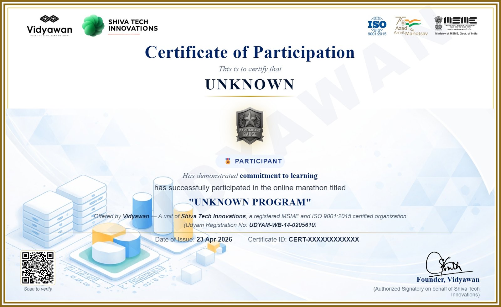
Students are awarded performance badges based on their quiz scores, task completion, and overall engagement.
Certificates You Will Receive
Verify Existing →Upon successful completion you receive a Government-Recognised Certificate from Vidyawan — a registered MSME enterprise (UDYAM-WB-14-0205610), governed under ISO 9001:2015 quality standards.
Why Vidyawan is Legit?
Know More →- MSME Registered — UDYAM-WB-14-0205610, Govt. of India
- ISO 9001:2015 Certified — Quality-controlled program delivery
- Verifiable Certificates — QR-code & ID-based online verification
- Rated 4.8★ — Trusted by 1000+ engineering students
- Real Leaderboards — Transparent, real-time performance tracking
- Offer Letter on Joining — Official document on enrollment
- Secure Payment — Powered by Razorpay gateway
- Verified Certificate on Completion
- Structured Tasks & Assignments
- Leaderboard & Performance Badges
- Offer Letter on Joining
- Email & WhatsApp Support
- Govt-Registered MSME (ISO Certified)
- Access to Free Simulators


Program Stats
| Enrolled | 500+ students |
| Rating | ★★★★★ 4.8/5 |
| Avg. Completion | 28 days |
| Certs Issued | 1000+ |


